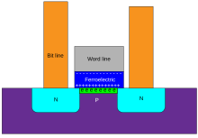
A ferroelectric field-effect transistor (Fe FET) is a type of field-effect transistor that includes a ferroelectric material sandwiched between the gate electrode and source-drain conduction region of the device (the channel). Permanent electrical field polarisation in the ferroelectric causes this type of device to retain the transistor's state (on or off) in the absence of any electrical bias.
FeFET based devices are used in FeFET memory - a type of single transistor non-volatile memory.
Description
In 1955, Ian Munro Ross filed a patent for a FeFET or MFSFET. Its structure was like that of a modern inversion channel MOSFET, but ferroelectric material was used as a dielectric/insulator instead of oxide. Use of a ferroelectric (triglycine sulfate) in a solid state memory was proposed by Moll and Tarui in 1963 using a thin film transistor. Further research occurred in the 1960s, but the retention characteristics of the thin film based devices was unsatisfactory. Early field effect transistor based devices used bismuth titanate (Bi4Ti3O12) ferroelectric, or Pb1−xLnxTiO3 (PLT) and related mixed zirconate/titanates (PLZT). In the late 1980 Ferroelectric RAM was developed, using a ferroelectric thin film as capacitor, connected to an addressing FET.
FeFET based memory devices are read using voltages below the coercive voltage for the ferroelectric.
Issues involved in realising a practical FeFET memory device include (as of 2006) : choice of a high permitivity, highly insulating layer between ferroelectric and gate; issues with high remanent polarisation of ferroelectrics; limited retention time (c. a few days, cf required 10 years).
Provided the ferroelectric layer can be scaled accordingly FeFET based memory devices are expected to scale (shrink) as well as MOSFET devices; however a limit of ~20 nm laterally may exist (the superparaelectric limit, aka ferroelectric limit). Other challenges to feature shrinks include : reduced film thickness causing additional (undesired) polarisation effects; charge injection; and leakage currents.
Research and development

In 2017 FeFET based non-volatile memory was reported as having been built at 22nm node using FDSOI CMOS (fully depleted silicon on insulator) with hafnium dioxide (HfO2) as the ferroelectric- the smallest FeFET cell size reported was 0.025 μm, the devices were built as 32Mbit arrays, using set/reset pulses of ~10ns duration at 4.2V - the devices showed endurance of 10 cycles and data retention up to 300C.
As of 2017 the startup Ferroelectric Memory Company is attempting to develop FeFET memory into a commercial device, based on hafnium dioxide. The company's technology is claimed to scale to modern process node sizes, and to integrate with contemporary production processes, i.e. HKMG, and is easily integrable into conventional CMOS processes, requiring only two additional masks.
See also
- Ferroelectric RAM, RAM that uses a ferroelectric material in the capacitor of a conventional DRAM structure
References
- Stefan Ferdinand Müller (2016). Development of HfO2-Based Ferroelectric Memories for Future CMOS Technology Nodes. BoD – Books on Demand. ISBN 9783739248943.
- Park et al. 2016, §1.1.1, p.3.
- ^ Park et al. 2016, §1.1.1, p.4.
- Park et al. 2016, § 1.1.2, p.6.
- ^ Zschech, Ehrenfried; Whelan, Caroline; Mikolajick, Thomas, eds. (2005), Materials for Information Technology: Devices, Interconnects and Packaging, Springer, pp. 157 –
- Khosla, Robin; Sharma, Deepak K.; Mondal, Kunal; Sharma, Satinder K. (2014-10-13). "Effect of electrical stress on Au/Pb (Zr0.52Ti0.48) O3/TiOxNy/Si gate stack for reliability analysis of ferroelectric field effect transistors". Applied Physics Letters. 105 (15): 152907. Bibcode:2014ApPhL.105o2907K. doi:10.1063/1.4897952. ISSN 0003-6951.
- ^ Dünkel, S. (Dec 2017), "A FeFET based super-low-power ultra-fast embedded NVM technology for 22nm FDSOI and beyond", 2017 IEEE International Electron Devices Meeting (IEDM), pp. 19.7.1–19.7.4, doi:10.1109/IEDM.2017.8268425, ISBN 978-1-5386-3559-9, S2CID 19624615
- Lapedus, Mark (16 Feb 2017), "What Are FeFETs?", semiengineering.com
- Park, Byung-Eun; Ishiwara, Hiroshi; Okuyama, Masanori; Sakai, Shigeki; Yoon, Sung-Min, eds. (2016), "Ferroelectric-Gate Field Effect Transistor Memories: Device Physics and Applications", Topics in Applied Physics, no. 131, Springer
Further reading
- Ishiwara, Hiroshi (2012), "FeFET and ferroelectric random access memories", Multifunctional Oxide Heterostructures, pp. 340–363, doi:10.1093/acprof:oso/9780199584123.003.0012, ISBN 978-0-19-958412-3