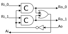

Within digital electronics, the DIMS (delay-insensitive minterm synthesis) system is an asynchronous design methodology making the least possible timing assumptions. Assuming only the quasi-delay-insensitive delay model the generated designs need little if any timing hazard testing. The basis for DIMS is the use of two wires to represent each bit of data. This is known as a dual-rail data encoding. Parts of the system communicate using the early four-phase asynchronous protocol.
The construction of DIMS logic gates comprises generating every possible minterm using a row of C-elements and then gathering the outputs of these using OR gates which generate the true and false output signals. With two dual-rail inputs the gate would be composed of four two-input C-elements. A three input gate uses eight three-input C-elements.
Latches are constructed using two C-elements to store the data and an OR gate to acknowledge the input once the data has been latched by attaching as its inputs the data output wires. The acknowledge from the forward stage is inverted and passed to the C-elements to allow them to reset once the computation has completed. This latch design is known as the 'half latch'. Other asynchronous latches provide a higher data capacity and levels of decoupling.
DIMS designs are large and slow but they have the advantage of being very robust.
- D. E. Muller, “Asynchronous logics and application to information processing,” Proc. Symp. Application of Switching Theory in Space Technology, H. Aiken and W. F. Main, Ed. , pp. 289-297, 1963.
Further reading
- Jens Sparsø, Steve Furber: "Principles of Asynchronous Circuit Design"; Kluwer, Dordrecht (2001); chapter 5.5.1. ISBN 0-7923-7613-7