This is an old revision of this page, as edited by Dicklyon (talk | contribs) at 01:42, 23 April 2011 (rm see also section, as only item is already linked in text). The present address (URL) is a permanent link to this revision, which may differ significantly from the current revision.
Revision as of 01:42, 23 April 2011 by Dicklyon (talk | contribs) (rm see also section, as only item is already linked in text)(diff) ← Previous revision | Latest revision (diff) | Newer revision → (diff)Baker clamp is a generic name for a class of electronic circuits that reduce the storage time of a switching bipolar junction transistor (BJT) by applying a nonlinear negative feedback through various kinds of diodes. The reason for slow turn-off times of saturated BJTs is the stored charge in the base. It must be removed before the transistor will turn off since the storage time is a limiting factor of using bipolar transistors and IGBTs in fast switching applications. The diode-based Baker clamps prevent the transistor from saturating and thereby accumulating a lot of stored charge.
Origin


The Baker clamp is named for Richard H. Baker, who described it in his 1956 technical report "Maximum Efficiency Switching Circuits." Many sources credit Baker's report for the two-transistor clamp circuit. Also in 1956, Baker described the circuit in a patent application; the 1961 issued patent, US 3,010,031, claims the use of the clamp in symmetrical flip-flop circuits. Similar clamp circuits are said to have been known before Baker's report.
Basic idea
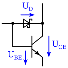
The Baker clamp introduces a nonlinear negative feedback into a common-emitter stage (BJT switch), with the purpose to avoid saturation by decreasing the gain near the saturation point. While the transistor is in active mode and it is far away enough from the saturation point, the negative feedback is turned off and the gain is maximal; when the transistor approaches the saturation point, the negative feedback gradually turns on, and the gain quickly drops. To decrease the gain, the transistor acts as a shunt regulator with regard to its own base–emitter junction: it diverts a part of the base current to ground by connecting a voltage-stable element in parallel to the base–emitter junction.
Implementation
The two-diode Baker clamp circuit is shown in the figure from Baker's patent and in many other publications. The feedback diode between the collector and the input limits the collector voltage to approximately VBE by diverting the excessive input current through the collector to ground. An additional silicon diode is connected in series with the base terminal to raise the effective input voltage; the clamp diode in the collector–base feedback is sometimes made from germanium to minimize the voltage drop across it. The base diode allows a Si diode clamp to be used with a Si transistor and keeps VCE around a diode drop and much greater than VCE(sat). Unfortunately, it turns off and creates a high-impedance return path when trying to turn the transistor off. Although the base charge has been minimized, it is now more difficult to draw charge out of the base.
A second base diode connected antiparallel to the base diode (D2 in Baker's schematic) will provide a low-impedance return path for removing stored base charge in the transistor. This three-diode circuit is still referred to as a Baker clamp by some sources, while others only call the two-diode circuit a Baker clamp.
A simple alternative to the Baker clamp is a single low-voltage diode from the collector to the base. To work well, the forward drop of the diode must be less than the base–emitter drop, so low-voltage-drop germanium and Schottky diodes can be used with silicon transistors (the forward voltage drop of a Schottky diode is much less than the VBE bias voltage of a silicon transistor and it switches rapidly). An alternative diode clamp circuit connects the diode to a junction of two base-bias resistors. The contemporary solution is to integrate the combination of a Schottky diode and transistor into one Schottky transistor. Some sources also refer to this configuration as a Baker clamp.
One drawback of the Baker clamp is its increased low voltage-output level (as in a Darlington transistor). In logic circuits, it decreases the noise immunity; in power applications, it increases the dissipated power.
References
- Simon S. Ang (1995). Power-switching Converters. Marcel Dekker. p. 340. ISBN 9780824796303.
- R. H. Baker (1956), "Maximum Efficiency Switching Circuits", MIT Lincoln Laboratory Report TR-110
-
Richard F. Shea (editor) (1957). Transistor circuit engineering. Wiley. p. 322.
{{cite book}}:|author=has generic name (help) - Ernst Bleuler (1964). Methods of Experimental Physics Vol. 2: Electronic Methods. Academic Press. ISBN 9780124759022.
-
William D. Roehr and Darrell Thorpe (editors) (1963). Switching transistor handbook. Motorola Semiconductor Products. p. 32.
{{cite book}}:|author=has generic name (help) - ^
Symmetrical Back-Clamped Transistor Switching Circuit, October 24, 1956
{{citation}}: Unknown parameter|country-code=ignored (help); Unknown parameter|inventor-first=ignored (help); Unknown parameter|inventor-last=ignored (help); Unknown parameter|issue-date=ignored (help); Unknown parameter|patent-number=ignored (help) -
Kyttälä, Teemu (2008), Solid State Guitar Amplifiers, p. 128,
Although invention of the Baker Clamp circuit is credited to Richard H. Baker (US Patent 3,010,031) it was already common knowledge in 1953 and described in transistor introductory papers that were written by Richard F. Shea.
- ^ Department of the Army (1963) , Basic Theory and Application of Transistors; Technical Manual 11-690, Dover, pp. 195–199
- Neil Chadderton and Dino Rosaldi (May 1996). "High Frequency DC-DC Conversion using High Current Bipolar Transistors: 400kHz Operation with Optimised Geometry Devices" (PDF). Zetex.
- Roehr, William D., ed. (2001), Rectifier Applications Handbook (PDF) (revision 2 ed.), ON Semiconductor Pages 175–176 describe a 3-diode "Baker clamp".
- Harry E. Thomas (1968). Handbook of transistors, semiconductors, instruments, and microelectronics. Prentice-Hall. p. 228.
- Paul Horowitz and Winfield Hill (1989), The Art of Electronics (Second ed.), Cambridge University Press, p. 908, ISBN 9780521370950